Ist das Ihr Unternehmen? Profil übernehmen
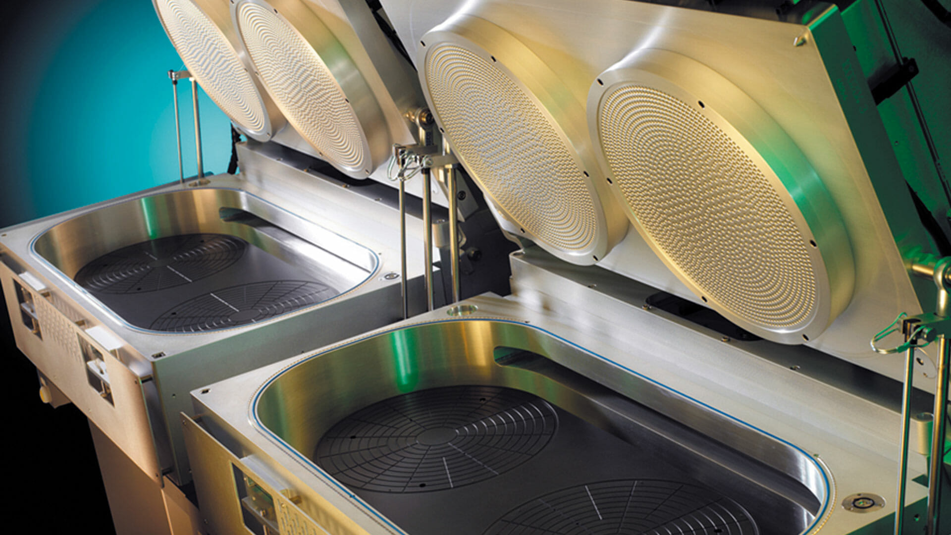
Entwickelt und fertigt Wafer-Verarbeitungssysteme für Dry Strip, Plasma Etch und Rapid Thermal Processing

Mattson Technology, Inc.
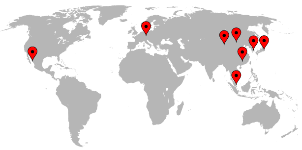
Fremont, CA (US) · Dornstadt (DE) · Dresden (DE) · Hsinchu, Taichung, Tainan (TW) · Hwaseong, Pyeongtaek, Icheon, Cheongju (KR) · Singapur (SG) · Tokio (JP)Neu auf Amplifa
Über Mattson Technology
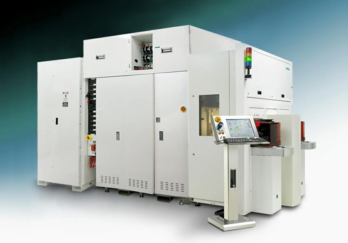
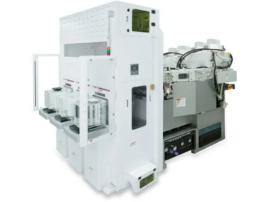
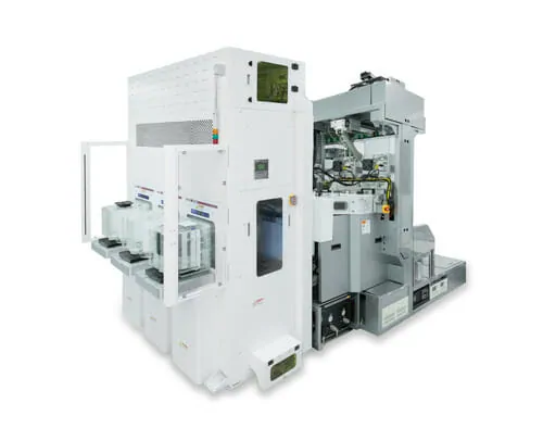
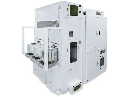
Mattson Technology, Inc. entwickelt, fertigt und unterstützt weltweit Halbleiter-Wafer-Verarbeitungsequipment für die Herstellung von integrierten Schaltungen. Das Portfolio umfasst Anlagen für Dry Strip (Photoresist-Entfernung), Plasma Etch mit induktiv gekoppeltem Plasma (ICP), Oberflächenbehandlung und ultraselktive Materialabtragung (Atomic Surface Engineering), Rapid Thermal Processing (RTP) mit beidseitiger Heizung sowie Millisecond Anneal. Bekannte Produktfamilien sind SUPREMA, paradigm E, Novyka, Helios, Millios und Aspen. Die Systeme kommen bei Herstellern von Memory-Chips (DRAM, 3D NAND), Foundry/Logic, CMOS-Bildsensoren, Power-ICs, MEMS, LED und Wafer Level Packaging zum Einsatz. Der 1988 in Fremont, Kalifornien gegründete Hersteller unterhält seinen Hauptsitz in Fremont sowie Designzentren und Fertigungsstätten in den USA und in Deutschland (Dornstadt); ein weltweites Vertriebs- und Servicenetz umfasst Standorte unter anderem in Dresden, Taiwan, Korea, Singapur und Japan.
- Standort
- Fremont, CA 94538, USA
- Verfahren
- Dry Strip (Photoresist Strip), Plasma Etch (ICP), Surface Treatment and Ultra-Selective Materials Removal (Atomic Surface Engineering, Novyka, Rapid Thermal Processing (RTP, double-side heating), Millisecond Anneal & Silicidation (Millios), Radical Enhanced Thermal Treatment (RETT, Interface Treatment), Kundensupport und globaler Service (Parts Support, Technical Support), Vertrieb und Service weltweit
- Werkstoffe
- Silizium-Wafer, Siliziumnitrid, Siliziumkarbid, Nickel-Silicide, Titan-Silicide, Kobalt-Silicide, Kupfer, High-k-Materialien
- Zertifikate
- ISO 9001:2015, ISO 14001:2015, ISO 45001:2018
- Gegründet
- 1988
- Branchen
- Halbleiterindustrie, Memory-Chip-Hersteller (DRAM, 3D NAND), Foundry/Logic, CMOS-Bildsensoren, Power IC, MEMS
- 01
Engineering und Design
- 02
Fertigung der Prozessmodule und Plattformen
- 03
Systemintegration und Test
- 04
Globale Installation
- 05
Service, Ersatzteile, Refurbishment und Obsoleszenz-Management
Standorte

Fremont, CA
USZentrale mit Fertigung und globalem Kundensupport
- Werkstoffe
- Silizium-Wafer, Photoresist, Silicide
- SUPREMA Dry Strip Systeme
- paradigm E Plasma Etch Systeme
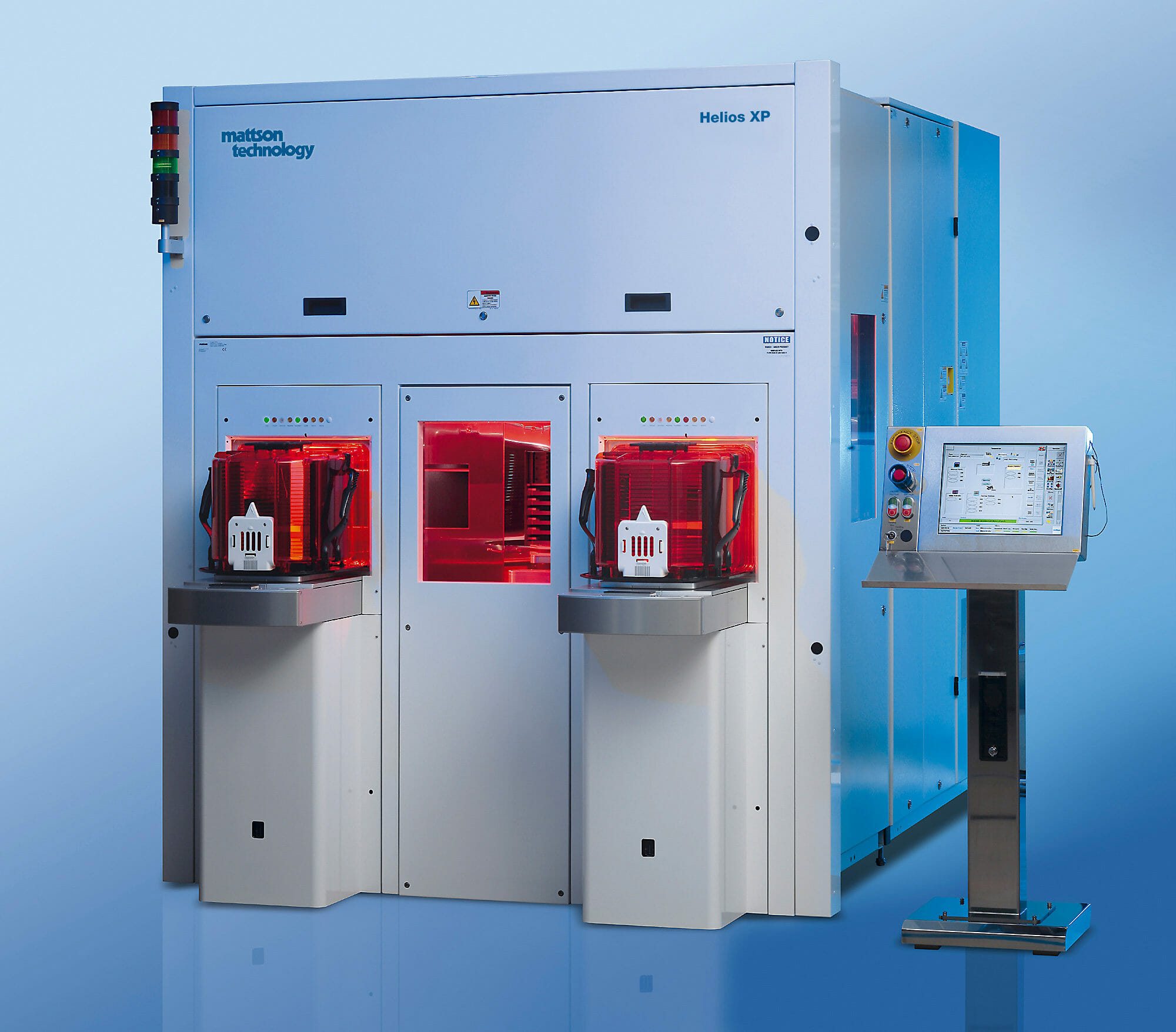
- Helios RTP Systeme
- Millios Millisecond Anneal Systeme
- Novyka Selective Etch Systeme
Dornstadt
DEFertigungswerk
- Werkstoffe
- Silizium-Wafer, Photoresist
- Fertigung von Wafer-Verarbeitungssystemen

Dresden
DEVertriebs- und Serviceniederlassung (Mattson International GmbH)
Singapore
SGGlobal Operations, Sales & Service
Hsinchu City
TWVertrieb und Service
Tokio
JPVertrieb und Service
Systeme und Anlagen
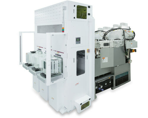
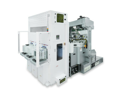
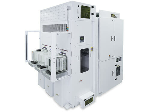
Einblicke in die Fertigung

Branchen
Verfahren & technische Grenzen
| Verfahren | Toleranz | Max. Bauteil | Gewicht | Losgröße | Werkstoffe |
|---|---|---|---|---|---|
| Dry Strip (Photoresist Strip)Oberfläche | – | – | – | – | Silizium-Wafer, Photoresist, Hardmask-Materialien, ARC |
| Plasma Etch (ICP)Oberfläche | – | – | – | – | Si, SiN/Oxid, Poly, ONO, BARC, Farbfilter/Lens-Materialien |
| Surface Treatment and Ultra-Selective Materials Removal (Atomic Surface Engineering, NovykaOberfläche | – | – | – | – | Dielektrika, Leitermaterialien |
| Rapid Thermal Processing (RTP, double-side heating)Wärmebehandlung | – | – | – | – | Silizium-Wafer, Nickel/Titan/Kobalt-Silicide |
| Millisecond Anneal & Silicidation (Millios)Wärmebehandlung | – | – | – | – | Silizium-Wafer, Nickel-Silicide, Titan-Silicide, High-k-Materialien |
| Radical Enhanced Thermal Treatment (RETT, Interface Treatment)Wärmebehandlung | – | – | – | – | – |
10 Anlagen & Maschinen
| Maschine | Hersteller / Modell | Anzahl | Arbeitsraum | Baujahr | Standort |
|---|---|---|---|---|---|
| ICP Plasma Etch System | Mattson Technology paradigm E XP | – | 200/300 mm Wafer (abgeleitet) | – | – |
| ICP PAD Etcher | Mattson Technology paradigm E PAD | – | – | – | – |
| Plasma Dry Strip System | Mattson Technology SUPREMA | – | – | – | – |
| Dry Strip / Etch Platform (200/300 mm Bridge Tool) | Mattson Technology Aspen III | – | 200 mm / 300 mm Wafer; warped wafers > 5 mm | – | – |
| Dry Strip System | Mattson Technology Aspen II | – | Wafer 100/150/200 mm; Temperaturbereich 100°C bis 250°C | – | – |
| Plasma Strip und Semi-Critical Etch System | Mattson Technology Alpine | – | – | – | – |
| Selective Etch System | Mattson Technology Novyka | – | – | – | – |
| RTP System (Double-Side Heating) | Mattson Technology Helios XP | – | 300 mm Wafer (abgeleitet); Temperaturbereich 200°C bis 1300°C | – | – |
| RTP System (200 mm) | Mattson Technology Helios C200 | – | 200 mm Wafer; Temperaturbereich 200°C bis 1300°C | – | – |
| Millisecond Anneal System (Argon Arc Lamp) | Mattson Technology Millios | – | Prozessbereich 250°C bis 1050°C; max. Temperatursprung 600°C; Emissivity 0,2 bis 0,9 | – | – |
Zusatzleistungen
Qualität
Mattson Technology arbeitet nach einem globalen Qualitätsmanagementsystem nach ISO 9001:2015 und ergänzt dies durch ISO 14001:2015 (Umwelt) und ISO 45001:2018 (Arbeitsschutz). Kontinuierliche Verbesserung, Ursachenanalyse und Lieferantenpartnerschaften sind Bestandteil des Systems.
| Nachweis | Mattson Technology (global) |
|---|---|
| ISO 9001:2015 | |
| ISO 14001:2015 | |
| ISO 45001:2018 |
Historie
- 1988
Gründung in Fremont, Kalifornien; Einstieg als führender Anbieter von Dry-Strip-Equipment, später Erweiterung um Plasma Etch, Rapid Thermal Anneal und Millisecond Anneal
- 1990
Einführung des Aspen II Systems
- 2023
Umstrukturierung als Corporation (Delaware)