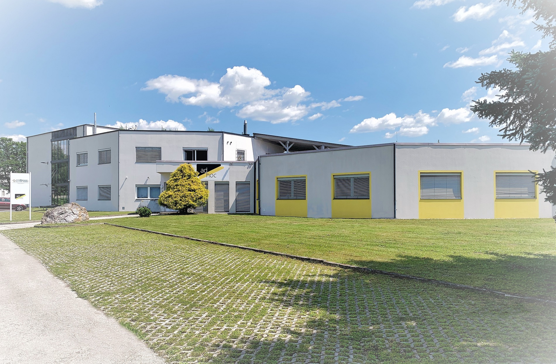
Development and production of electronic systems, assemblies and embedded software from prototype to small series

adhoc Hard- und Software GmbH & Nfg KG
Klagenfurt am Wörthersee, AustriaNew on Amplifa
About adhoc Hard- und Software
adhoc Hard- und Software GmbH & Nfg KG was founded in 1986 as a technical office and has been developing and producing electronic systems and equipment at its location in Klagenfurt am Wörthersee since 1995. The range of services includes hardware development (circuit design, simulation, PCB design according to IPC standards), software development (microcontroller firmware, FPGA/VHDL, PC, mobile and web applications, HMI, AI systems) as well as IoT development for connected embedded systems. In its own manufacturing facility, PCBs are populated semi- and fully automatically (SMD), including solder paste printing, selective soldering, QFN/BGA rework, cable assembly and device assembly. Lot sizes range from prototypes and micro series starting at 2 pieces to small series of up to 20,000 pieces; large series are implemented with external partners. A dedicated test engineering department operates automated functional testing, measurement stations for digital technology, audio and RF measurement technology as well as its own EMC measurement chamber. Typical fields of application include medical technology, industrial metrology, automation, apparatus engineering as well as control and regulation technology.
- Site
- Klagenfurt am Wörthersee
- Processes
- PCB population (semi- and fully automatic, SMD), QFN and BGA rework, Cable assemblies, Selective soldering, Screen and stencil printing (solder paste printing), 3-axis milling (mechatronics machining center, housing/prototype parts), Device assembly, Automated functional testing
- Materials
- Printed circuit boards, Glass, ceramics, metal, Cables & connectors
- Certificates
- IPC standards (PCB design), EMC measurement chamber in-house, Automated functional testing, ISO 9001
- Founded
- 1986
- Industries
- Medical technology, Industrial metrology, Automation, Consumer electronics, Apparatus engineering, Control and regulation technology
- 01
Hardware development (circuit design, simulation, PCB design according to IPC)
- 02
Software & firmware development (microcontroller, FPGA/VHDL)
- 03
Mechanical design (CAD, 3-axis milling)
- 04
Prototype development (EVT, DVT, PVT)
- 05
Solder paste printing (screen and stencil printing)
- 06
Semi- and fully automatic SMD population
- 07
Selective soldering
- 08
QFN/BGA rework (reballing, dispensing)
- 09
Cable assembly
- 10
Automated functional testing and EMC measurements
- 11
Device assembly
- 12
Product service (maintenance, repair)
Materials & Processes
Printed circuit boards
Custom PCB layouts and electronic assemblies according to IPC standards as the basis of electronics manufacturing.
Glass, ceramics, metal
As substrate materials for screen and stencil printing up to a material thickness of 30 mm.
Cables & connectors
Processed into assembled cable harnesses with crimping, labeling and final testing according to customer specification.
Locations
Klagenfurt am Wörthersee
ATHeadquarters: development, production, sales
- Lot size
- Prototypes, micro series from 2 pcs., small series up to 20,000 pcs.
- Materials
- Printed circuit boards, glass, ceramics, metal, cables, connectors
- Essemtec Fox SMD population system
- Fine-pitch and BGA microplacer
- Rework system (BGA/QFN, seven functions incl. reballing)
- Semi-automatic SMD population system
- Manual screen and stencil printer (up to 30 mm material thickness)
- Selective soldering system
- Mechatronics machining center with 3-axis milling machine
- Audio measurement station (Audio Precision)
- EMC measurement chamber
- Thermography systems
- Automated chip characterization
Products & Assemblies
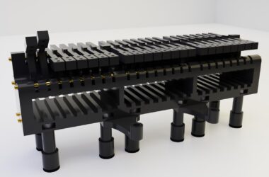
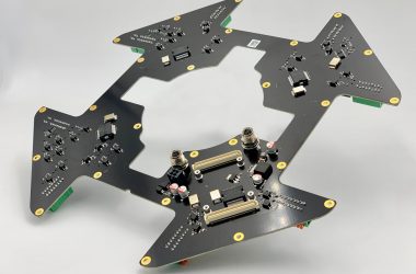

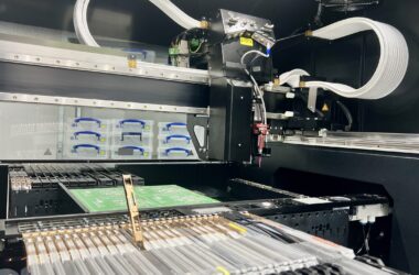
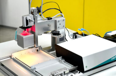
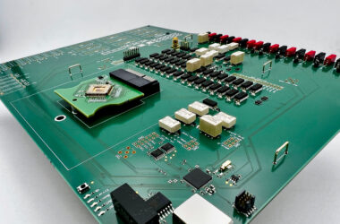
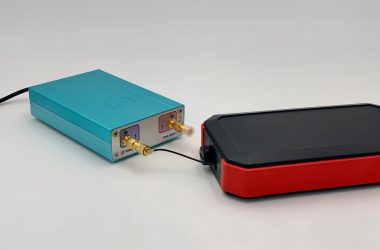
Inside the production
Industries
Processes & technical limits
| Processes | Tolerance | Max. part | Weight | Lot size | Materials |
|---|---|---|---|---|---|
| PCB population (semi- and fully automatic, SMD)Assembly | – | – | – | 2 pcs. (micro series) – 20,000 pcs. (small series, large series | – |
| QFN and BGA reworkAssembly | Pad spacing >= 0.3 mm (BGA/QFN placement) | – | – | – | – |
| Cable assembliesJoining | – | – | – | – | Cables, Connectors |
| Selective solderingJoining | – | – | – | small series – medium series | – |
| Screen and stencil printing (solder paste printing)Assembly | – | Material thickness up to 30 mm | – | – | Printed circuit boards, Glass, Ceramics, Metal |
| 3-axis milling (mechatronics machining center, housing/prototype parts)Machining | – | – | – | – | – |
| Device assemblyAssembly | – | – | – | – | – |
| Automated functional testingTesting | – | – | – | – | – |
| Electronic measurement and test engineering (digital 0-500 MHz, audio 10 Hz-200 kHz, RF 0-2 GHz,Testing | – | – | – | – | – |
| Fully automated chip characterization and verificationTesting | – | – | – | – | – |
| Hardware development (circuit design, simulation, PCB design according to IPC)Engineering | – | – | – | – | – |
| Software development (microcontroller, FPGA/VHDL, PC/mobile, web/HMI, AI)Engineering | – | – | – | – | – |
| Mechanical design (CAD)Engineering | – | – | – | – | – |
| Prototype development and production of prototypes & seriesAssembly | – | – | – | – | – |
| IoT development (connected embedded systems)Engineering | – | – | – | – | – |
9 Anlagen & Maschinen
| Machine | Manufacturer / model | Quantity | Working area | Year built | Site |
|---|---|---|---|---|---|
| SMD population system | Essemtec Fox | 1 | – | – | Klagenfurt am Wörthersee |
| Fine-pitch and BGA microplacer | – | 1 | – | – | Klagenfurt am Wörthersee |
| Rework system (BGA/QFN rework station) | – | 1 | – | – | Klagenfurt am Wörthersee |
| Mechatronics machining center with 3-axis milling machine | – | 1 | – | – | Klagenfurt am Wörthersee |
| Semi-automatic SMD population system | – | 1 | – | – | Klagenfurt am Wörthersee |
| Manual screen and stencil printer | – | 1 | Material thickness up to 30 mm | – | Klagenfurt am Wörthersee |
| Selective soldering system | – | 1 | – | – | Klagenfurt am Wörthersee |
| Audio measurement station | Audio Precision | 1 | – | – | Klagenfurt am Wörthersee |
| EMC measurement chamber | – | 1 | – | – | Klagenfurt am Wörthersee |
Additional services
Quality & Metrology and Test Engineering
All measuring and testing equipment is available in-house, from an Audio Precision audio measurement station to instruments for digital technology (0–500 MHz), audio technology (10 Hz–200 kHz) and high frequency (0–2 GHz), up to its own EMC measurement chamber. A dedicated test engineering department develops and produces measurement and test systems for automated verification of hardware components during commissioning.
| Evidence | Klagenfurt am Wörthersee |
|---|---|
| IPC standards (PCB design) | |
| EMC measurement chamber in-house | |
| Automated functional testing | |
| ISO 9001 |
Company History
- 1986
Founded as a technical office for consulting and expert assessment services
- 1995
Relocation of headquarters to Klagenfurt am Wörthersee; expansion into development and production of electronic systems and equipment