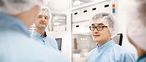
Development and manufacture of MOCVD and CVD deposition systems for compound semiconductors and 2D nanomaterials

AIXTRON SE
Herzogenrath (3 sites) · Cambridge, UK · Santa Clara, USA · Shanghai · Tokyo · Hwaseong, South Korea · Hsinchu, Taiwan · Kulim, MalaysiaNew on Amplifa
About AIXTRON
AIXTRON SE is a leading supplier of deposition systems for the semiconductor industry. Founded in 1983 as a spin-off of RWTH Aachen and headquartered in Herzogenrath, the company develops and manufactures MOCVD systems (Metal-Organic Chemical Vapor Deposition) with Planetary Reactor and Close Coupled Showerhead technology as well as SiC-CVD systems based on the warm-wall Planetary Reactor principle. The product portfolio includes systems for high-throughput epitaxy of 150/200 mm wafers for SiC power electronics, GaN power & RF, and GaAs/InP-based optoelectronics and RF applications, complemented by (PE)CVD systems for graphene, carbon nanotubes and 2D nanomaterials. To date, more than 3,000 deposition systems have been delivered worldwide. Customers come from LED and display technology, data transmission, sensor technology, power electronics and research, including IQE, Lumentum, Epistar, Infineon, Fraunhofer Institutes and universities. In addition to its headquarters in Herzogenrath with a 16,000 m² R&D center, AIXTRON maintains branches in Cambridge (UK), Santa Clara (USA) and several locations in Asia.
- Site
- Herzogenrath
- Processes
- MOCVD (Metal-Organic Chemical Vapor Deposition) for compound semiconductors (Planetary Reactor /, SiC-CVD (warm-wall Planetary Reactor principle / VPE) for SiC epitaxy, Plasma-Enhanced Chemical Vapor Deposition (PE)CVD, Thermal CVD for 2D nanomaterials, MOCVD high-throughput epitaxy 150/200 mm for SiC power electronics, MOCVD high-throughput epitaxy 150/200 mm for GaN power & RF, MOCVD for high-volume production of GaAs/InP materials, MOCVD system manufacturing (manufacturer of deposition systems, no contract manufacturing)
- Materials
- Gallium arsenide (GaAs), Indium phosphide (InP), Gallium nitride (GaN), Aluminum gallium nitride (AlGaN), Silicon carbide (SiC), Silicon (Si substrates), Sapphire (substrate), Graphene
- Certificates
- ISO 9001:2015 (DQS), ISO 50001:2018, ISO 14001:2015, ISO 45001:2018, EN ISO/IEC 27001:2022, CE / TÜV / ETL / UL
- Industries
- Semiconductor industry, LED and display technology, Power electronics (SiC/GaN), Optoelectronics and lasers, RF electronics, Data transmission
- 01
Research & Development
- 02
System design (engineering)
- 03
Manufacture and assembly of deposition systems
- 04
Commissioning and installation at the customer
- 05
Maintenance, upgrades and spare parts supply
- 06
Training at the Training Center & Lab
Technologies & Material Classes
MOCVD (Planetary Reactor / Close Coupled Showerhead)
Deposition of III-V compound semiconductors such as GaAs, InP, GaN and AlGaN for LED, laser and RF applications.
SiC-CVD (warm-wall Planetary Reactor principle)
Epitaxy of silicon carbide for 150/200 mm power electronics devices.
(Plasma-Enhanced) Chemical Vapor Deposition
Deposition of graphene, carbon nanotubes and 2D nanomaterials using thermal and plasma-assisted processes.
Gallium arsenide (GaAs)
Material for high-volume production of optoelectronic and RF devices.
Indium phosphide (InP)
Material for high-volume production of optoelectronic and RF devices.
Gallium nitride (GaN)
Epitaxy for GaN power & RF applications, including GaN-on-Si for micro-LED displays.
Aluminum gallium nitride (AlGaN)
Layer material for GaN power electronics and RF applications.
Silicon carbide (SiC)
Material for SiC power electronics in electromobility and energy management.
Silicon (Si substrates)
Substrate material for GaN-on-Si processes.
Sapphire (substrate)
Substrate material for LED epitaxy.
Graphene
2D nanomaterial for future computer chips.
Carbon nanotubes/wires
Nanomaterial with unique electronic properties.
Sites
Herzogenrath
DEHeadquarters, R&D center (16,000 m²), system manufacturing, Training Center & Lab
- Materials
- GaAs, InP, GaN, AlGaN, SiC
- G10-SiC MOCVD batch reactor (9x150 mm & 6x200 mm)
- G10-GaN MOCVD cluster system (3 process chambers)
- G10-AsP fully automated MOCVD Planetary Reactor
- AIX G5+ C Planetary Reactor
- AIX 2800G4-TM (IC2) Planetary Reactor
- AIX G5 WW C SiC VPE reactor
Cambridge (UK)
GBR&D and MOCVD system manufacturing (Close Coupled Showerhead)
- Materials
- GaAs, GaN
- CCS Flip Top Reactor (R&D system)
Santa Clara (USA)
USBranch office and service center
Shanghai
CNSales and service center
Tokyo
JPSales and service center
Hwaseong (Gyeonggi-do)
KRSales and service center
Hsinchu
TWSales and service center
Kulim (Kulim Hi-Tech Park)
MYBranch office
Deposition Systems
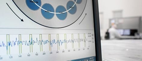
Inside the production
Industries
Processes & technical limits
| Processes | Tolerance | Max. part | Weight | Lot size | Materials |
|---|---|---|---|---|---|
| MOCVD (Metal-Organic Chemical Vapor Deposition) for compound semiconductors (Planetary Reactor /Surface | – | – | – | – | III-V compound semiconductors, GaAs, InP, GaN, SiC, AlGaN |
| SiC-CVD (warm-wall Planetary Reactor principle / VPE) for SiC epitaxySurface | – | – | – | – | SiC |
| Plasma-Enhanced Chemical Vapor Deposition (PE)CVDSurface | – | – | – | – | Graphene, Carbon nanotubes, 2D nanomaterials |
| Thermal CVD for 2D nanomaterialsSurface | – | – | – | – | Graphene, Carbon nanotubes/wires, 2D nanomaterials |
| MOCVD high-throughput epitaxy 150/200 mm for SiC power electronicsSurface | – | – | – | – | SiC |
| MOCVD high-throughput epitaxy 150/200 mm for GaN power & RFSurface | – | – | – | – | GaN, AlGaN |
| MOCVD for high-volume production of GaAs/InP materialsSurface | – | – | – | – | GaAs, InP |
| MOCVD system manufacturing (manufacturer of deposition systems, no contract manufacturing)Engineering | – | – | – | – | – |
8 Anlagen & Maschinen
| Machine | Manufacturer / model | Quantity | Working area | Year built | Site |
|---|---|---|---|---|---|
| MOCVD batch reactor (dual wafer size) | AIXTRON G10-SiC | – | 9x150 mm & 6x200 mm wafers | – | Herzogenrath |
| MOCVD cluster system (3 process chambers) | AIXTRON G10-GaN | – | 8x150 mm / 5x200 mm wafers | – | Herzogenrath |
| MOCVD Planetary Reactor (fully automated, C2C) | AIXTRON G10-AsP | – | 75/100/150/200 mm wafers, 2x25-wafer cassettes | – | Herzogenrath |
| MOCVD Planetary Reactor | AIXTRON AIX G5+ C | – | 8x150 mm / 5x200 mm | – | Herzogenrath |
| MOCVD R&D system (Close Coupled Showerhead Flip Top Reactor) | AIXTRON CCS Flip Top | – | 3x2", 6x2", 19x2", 5x4", 1x8" and other configurations | – | Cambridge (UK) |
| MOCVD Planetary Reactor (mass production GaAs/InP) | AIXTRON AIX 2800G4-TM (IC2) | – | 15x4" / 8x6" | – | Herzogenrath |
| SiC VPE reactor (warm-wall Planetary Reactor) | AIXTRON AIX G5 WW C | – | 8x150 mm | – | Herzogenrath |
| R&D center | AIXTRON | – | 16,000 m² usable floor space | 2010 | Herzogenrath |
Additional services
Quality Guarantee
In 1994, AIXTRON set an industry benchmark with its ISO 9001 certification and continuously expands the management system with ISO 50001, ISO 14001 and ISO 45001. Systems meet CE conformity as well as TÜV and ETL certification; most assemblies are UL-listed.
| Evidence | Herzogenrath |
|---|---|
| ISO 9001:2015 (DQS) | |
| ISO 50001:2018 | |
| ISO 14001:2015 | |
| ISO 45001:2018 | |
| EN ISO/IEC 27001:2022 | |
| CE / TÜV / ETL / UL |
History
- 1983
Founded by Dr. Holger Jürgensen and Dr. Meino Heyen, employees of the Institute of Semiconductor Technology at RWTH Aachen.
- 1985
Commissioning of the first AIXTRON MOCVD system.
- 1989
Exclusive license from Philips for the Planetary Reactor technology.
- 1990
Delivery of the first MOCVD multi-wafer system.
- 1994
ISO 9001 certification; first deposition system for manufacturing blue LEDs.
- 1997
IPO on the Frankfurt Stock Exchange (Neuer Markt/TecDAX).
- 1999
Acquisition of the Thomas Swan Scientific Equipment Division (AIXTRON Ltd, CCS technology) and of EPIGRESS AB (SiC-CVD).
- 2005
Acquisition of Genus, Inc. (USA) with ALD technology.
- 2007
Acquisition of Nanoinstruments Ltd. (UK), expansion into (PE)CVD nanotechnology.
- 2010
Conversion into an SE; commissioning of the 16,000 m² R&D center in Herzogenrath; launch of the G5 and CRIUS II system generations.
- 2011
Delivery of the 2,000th MOCVD system to Changelight Co., Ltd.
- 2012
Opening of the Training Center & Lab in Suzhou, China.
- 2013
30th anniversary; AIX G5+ Planetary Reactor awarded the CS Industry Award and Aurora Award.
- 2017
Sale of the ALD/CVD product line for memory chips; dena Energy Efficiency Award; focus of the product portfolio.
- 2020
AIXTRON becomes part of the MDAX.
- 2022
AIXTRON becomes part of the EUROSTOXX 600; OLED business (APEVA) discontinued.
- 2023
G10-GaN and G10-AsP launch completes the G10 product family.
- 2024
Opening of the innovation center in Herzogenrath.