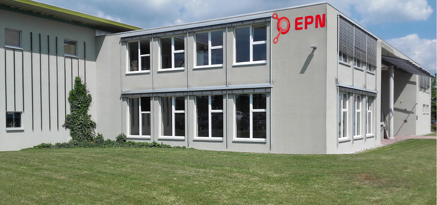
Manufacturer of single- to multilayer PCBs, HDI, IMS and heavy copper PCBs, manufactured in Neustadt an der Orla.

EPN Electroprint GmbH
Neustadt an der OrlaNew on Amplifa
About EPN Electroprint
EPN Electroprint GmbH is a PCB manufacturer founded in 1990, headquartered in Neustadt an der Orla in Thuringia. The company produces single-sided and double-sided PCBs, multilayer PCBs with up to 12 layers, HDI PCBs with Sequential Build Up, IMS PCBs with metal core, RF and microwave PCBs as well as heavy copper parts for power electronics. The value chain includes design and co-design support, prototyping, series production, quick-turn delivery (QTA), impedance control, solder masks, various final finishes (HAL, ENIG, immersion tin and silver, electrolytic Ni/Au, ENEPIG) as well as laboratory analysis and product certification (CoC, FAI, PPAP). Used materials include FR4 standard and lead-free laminates, mid- and high-Tg materials, high-speed and high-frequency laminates (Isola FR408HR, Rogers RO4350B) as well as thermal base materials (Ventec VT-4B3/4B5/4B7) with aluminium core. The company supplies industries such as industrial and process automation, electromobility, renewable energies, automotive, safety, sensor and lighting technology as well as consumer electronics. Since January 2019, EPN has been part of the PCB Division of the Finmasi Group; production takes place on 4,500 m² of manufacturing floor space in Germany.
- Site
- Neustadt an der Orla
- Processes
- Manufacture of single-sided PCBs, Manufacture of double-sided PCBs, Multilayer PCBs, HDI PCBs / Sequential Build Up (SBU), Insulated Metal Substrate (IMS) / metal-core PCBs, RF and microwave PCBs, Heavy copper technology / High-Power Heavy Copper, Semi-flexible PCBs
- Materials
- FR4 standard and lead-free, Iteq IT140, Nanya NP-155F, ILM R1 (GF112), Iteq IT158, Shengyi Autolad1, Shengyi S1000H, Panasonic R1755M
- Certificates
- ISO 9001:2015, ISO 14001:2015, ISO 50001:2018, UL94-V-0 (with UL796 DSR extension), UL94-V-0 / UL796 DSR, IPC-A-600 Class 2 / IPC-6012
- Founded
- 1990
- Industries
- Industrial automation, Process automation, Electromobility, Renewable energies, Safety technology, Sensor technology
- 01
Design / co-design support (Gerber review, stack-up calculation)
- 02
Prototyping (also quick-turn delivery QTA)
- 03
Photo printing (LDI/LED exposure)
- 04
Drilling (mechanical and laser) and through-hole plating
- 05
Multilayer pressing
- 06
Electroplating and final finishes
- 07
Solder mask (curtain coating, screen printing, spray process)
- 08
Milling and mechanical machining
- 09
E-test, impedance measurement, laboratory analysis and product certification
Materials and Processes
FR4 standard and lead-free (Iteq IT140, Nanya NP-155F, ILM R1)
Standard and lead-free laminates for single- and double-sided PCBs with an excellent price-performance ratio.
Mid-Tg materials (Iteq IT158 Tg 160°C, Shengyi S1000H Tg 150°C, Panasonic
Epoxy resins with elevated glass transition temperature for lead-free soldering processes.
High-Tg materials (Iteq IT180ATC, Iteq IT180TC, Nanya NP-170, Tg 180°C)
For thermally demanding applications and HDI build-ups.
Isola FR408HR
High-speed laminate for signal transmission with impedance control.
Rogers RO4350B
High-frequency laminate on hydrocarbon/ceramic basis for RF and microwave applications.
Ventec VT-4B3 / VT-4B5 / VT-4B7 (3–7 W/mK)
Insulated metal substrates with thermal conductivity up to 7 W/mK for effective heat dissipation, partly with 6061 aluminium core.
Heavy Copper
Heavy copper technology based on Iteq IT-158, Panasonic R1755M and Iteq IT-180ATC for power and high-power applications.
Final finishes: HAL lead-free/leaded, ENIG, immersion tin, immersion silver,
Various finishes depending on assembly process, market sector and wire-bondability.
Solder mask, peelable and special inks
Polymer protective ink in all market types and colours (green, blue, white, black, yellow, red), glossy or matte, applied by curtain coating, screen printing or spray process.
Site
Neustadt an der Orla
DEProduction and administration (headquarters)
- Lot size
- Prototype to series
- Materials
- FR4, High-Tg, IMS/aluminium, high-frequency, heavy copper
- LDI/LED exposure systems
- High-performance drilling machines
- 6-shelf LAUFFER multilayer press
- Fully automatic E-tester ATG A7a
- Electroplating line
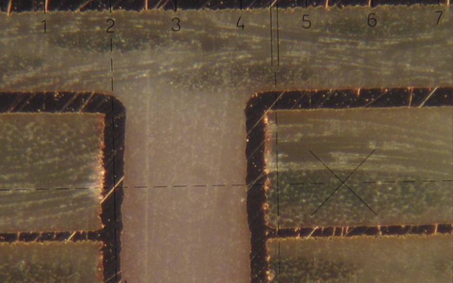
- Laboratory (cross-sections, XRF, thermal stress tests)
Parts
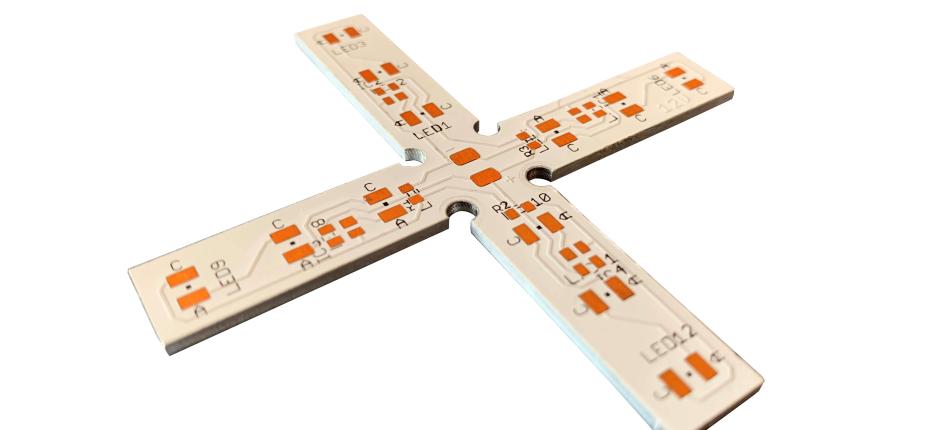
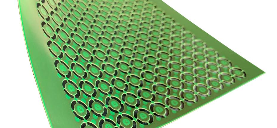
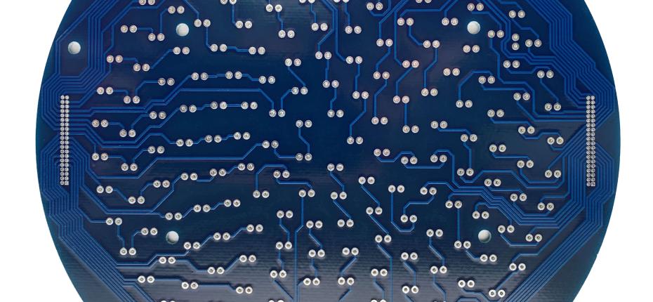
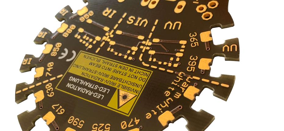
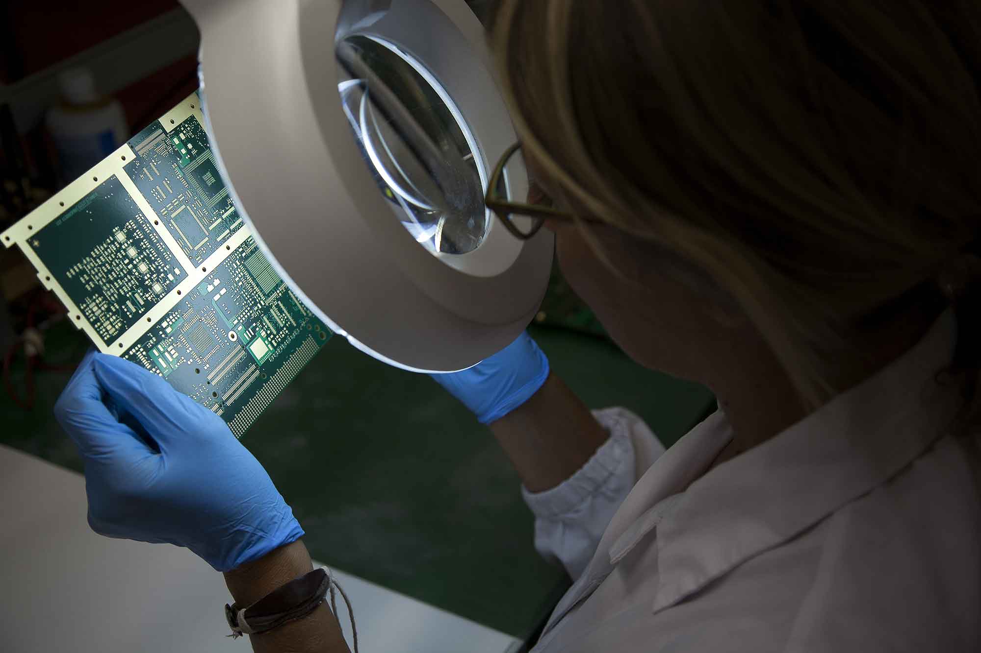
Inside the production
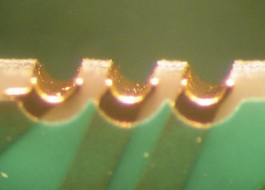
Industries
Processes & technical limits
| Processes | Tolerance | Max. part | Weight | Lot size | Materials |
|---|---|---|---|---|---|
| Manufacture of single-sided PCBsPCB manufacturing | – | – | – | – | FR4, IMS/base material |
| Manufacture of double-sided PCBsPCB manufacturing | – | – | – | – | FR4 standard and lead-free, FR4 0.2mm, Black FR4, Mid-Tg, High-Tg |
| Multilayer PCBsPCB manufacturing | – | – | – | up to 12 layers | FR4 standard and lead-free, Mid-Tg, High-Tg, High-speed, High-frequency |
| HDI PCBs / Sequential Build Up (SBU)PCB manufacturing | – | – | – | – | FR4 High-Tg, Iteq IT180A |
| Insulated Metal Substrate (IMS) / metal-core PCBsPCB manufacturing | – | – | – | – | Ventec VT-4B3 3 W/mK, Ventec VT-4B5 4.2 W/mK, Ventec VT-4B7 7 W/mK, 6061 aluminium |
| RF and microwave PCBsPCB manufacturing | – | – | – | – | Rogers RO4350B |
| Heavy copper technology / High-Power Heavy CopperPCB manufacturing | – | – | – | – | Iteq IT-158, Panasonic R1755M, Iteq IT-180ATC |
| Semi-flexible PCBsPCB manufacturing | – | – | – | – | FR4 0.2mm |
| Laser and mechanical drilling (blind vias, microvias)PCB manufacturing | – | – | – | – | FR4, IMS |
| Via fill technology (copper and resin fill, filled & capped vias, reverse build-up)PCB manufacturing | – | – | – | – | Copper, Resin (conductive/non-conductive) |
| Copper plating of hole walls (through-hole plating PTH)Surface treatment | – | – | – | – | Copper |
| Electroplating line (electrolytic copper deposits)Surface treatment | – | – | – | – | Copper |
| HAL leaded (hot air solder levelling tin-lead)Surface treatment | – | – | – | – | Tin-lead solder |
| HAL lead-free (hot air solder levelling lead-free)Surface treatment | – | – | – | – | Tin (lead-free) |
| ENIG (electroless nickel-gold)Surface treatment | – | – | – | – | Nickel, Gold |
| Immersion tinSurface treatment | – | – | – | – | Tin |
| Immersion silverSurface treatment | – | – | – | – | Silver |
| Electrolytic nickel-gold (bondable gold)Surface treatment | – | – | – | – | Nickel, Gold |
| ENEPIG (electroless nickel/palladium/gold)Surface treatment | – | – | – | – | Nickel, Palladium, Gold |
| OSP (organic protective coating)Surface treatment | – | – | – | – | – |
| Solder mask (all colours: green, blue, white, black, yellow, red; glossy/matte), peelable andSurface treatment | – | – | – | – | Solder mask (polymeric material) |
| LDI exposure technology / LED exposure (inner-layer and outer-layer photo printing, solder mask)PCB manufacturing | – | – | – | – | – |
| Curtain coating, screen printing and spray processes for solder maskSurface treatment | – | – | – | – | – |
| Lamination / multilayer pressingJoining | – | – | – | – | FR4 prepreg/laminate |
| Impedance control / impedance-controlled PCBsTesting | – | – | – | – | High-frequency laminates, High-speed laminates |
| Electrical test (E-test)Testing | – | – | – | – | – |
| Laboratory analysis: cross-sections, thermal stress tests (IPC TM650 2.6.8 at 288 °C, IPC TM650Testing | – | – | – | – | – |
| Milling (mechanical machining of PCBs)Machining | – | – | – | – | FR4, IMS/aluminium |
| Heat sink installationAssembly | – | – | – | – | – |
| Design support / co-design (Gerber review, stack-up calculation)Engineering | – | – | – | – | – |
| Prototyping and quick-turn delivery (QTA)PCB manufacturing | – | – | – | – | – |
| Busbar assembly (for power applications)PCB manufacturing | – | – | – | – | Copper |
5 Anlagen & Maschinen
| Machine | Manufacturer / model | Quantity | Working area | Year built | Site |
|---|---|---|---|---|---|
| Fully automatic E-tester | ATG A7a | 1 | – | 2018 | Neustadt an der Orla |
| Multilayer press (6 shelves) | LAUFFER | 1 | – | 2022 | Neustadt an der Orla |
| High-performance drilling machines | – | several | – | 2021 | Neustadt an der Orla |
| Electroplating line | – | 1 | – | 2002 | Neustadt an der Orla |
| LDI exposure system (later LED exposure) | – | – | – | 2014/2021 | Neustadt an der Orla |
Additional services
Quality and Standards
Production is carried out to IPC-A-600 Class 2 and IPC-6012 (rigid); the integrated management system is certified to ISO 9001, ISO 14001 and ISO 50001. In its own laboratory, cross-sections, thermal stress tests (IPC TM650 2.6.8/2.6.27), X-ray fluorescence analyses and statistical process control (SPC) are performed.
| Evidence | Neustadt an der Orla |
|---|---|
| ISO 9001:2015 | |
| ISO 14001:2015 | |
| ISO 50001:2018 | |
| UL94-V-0 / UL796 DSR | |
| IPC-A-600 Class 2 / IPC-6012 |
Company History
- 1990
Founding of EPN Electroprint GmbH in Neustadt an der Orla
- 2002
Relocation to the new company building In den Grupenäckern 2 (10,000 m² plot, 4,500 m² production area) and installation of a new electroplating line
- 2003
Start of multilayer PCB production
- 2006
Certification to ISO 9001 and ISO 14001
- 2011
Thuringian State Prize for Quality
- 2014
Introduction of LDI exposure technology
- 2016
Purchase of the adjacent 5,000 m² property
- 2017
Start of production of impedance-controlled PCBs
- 2018
Commissioning of the fully automatic E-tester ATG A7a
- 2019
Integration into the PCB Division of the Finmasi Group
- 2021
Switch to LED exposure technology, installation of new high-performance drilling machines and ISO 50001 certification
- 2022
Installation of a 6-shelf LAUFFER multilayer press; LED exposure technology for the solder mask
- 2023
Expansion of the portfolio to heavy copper technology, high-power solutions and custom designs