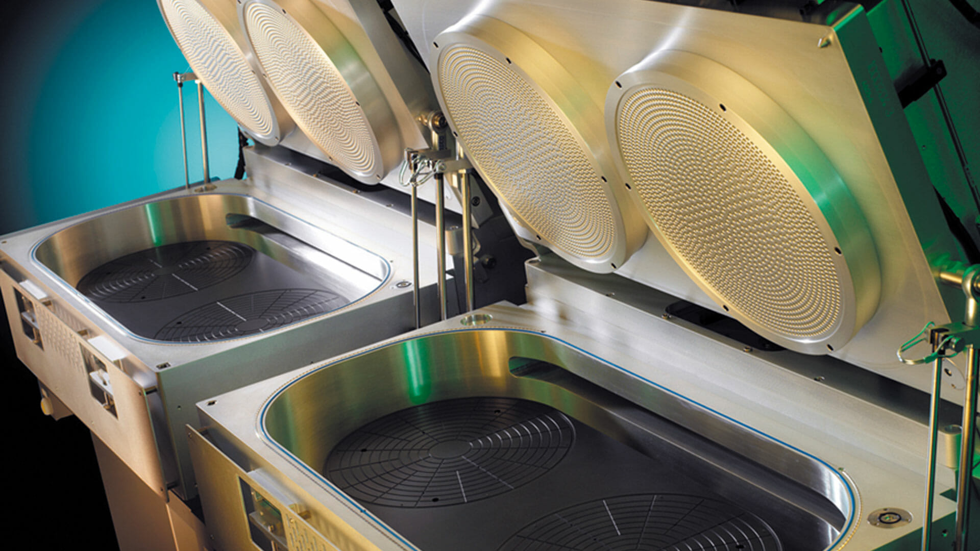
Develops and manufactures wafer processing systems for Dry Strip, Plasma Etch and Rapid Thermal Processing

Mattson Technology, Inc.
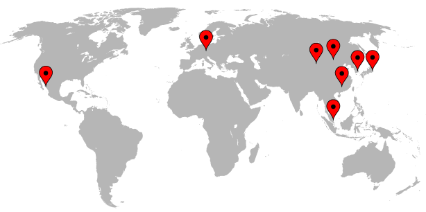
Fremont, CA (US) · Dornstadt (DE) · Dresden (DE) · Hsinchu, Taichung, Tainan (TW) · Hwaseong, Pyeongtaek, Icheon, Cheongju (KR) · Singapore (SG) · Tokyo (JP)New on Amplifa
About Mattson Technology
Mattson Technology, Inc. develops, manufactures and supports semiconductor wafer processing equipment worldwide for the production of integrated circuits. The portfolio includes systems for Dry Strip (photoresist removal), Plasma Etch with inductively coupled plasma (ICP), surface treatment and ultrasensitive material removal (Atomic Surface Engineering), Rapid Thermal Processing (RTP) with dual-side heating as well as Millisecond Anneal. Well-known product families include SUPREMA, paradigm E, Novyka, Helios, Millios and Aspen. The systems are used by manufacturers of memory chips (DRAM, 3D NAND), Foundry/Logic, CMOS image sensors, Power ICs, MEMS, LED and Wafer Level Packaging. Founded in 1988 in Fremont, California, the manufacturer maintains its headquarters in Fremont as well as design centers and manufacturing facilities in the USA and Germany (Dornstadt); a worldwide sales and service network includes locations among others in Dresden, Taiwan, Korea, Singapore and Japan.
- Site
- Fremont, CA 94538, USA
- Processes
- Dry Strip (Photoresist Strip), Plasma Etch (ICP), Surface Treatment and Ultra-Selective Materials Removal (Atomic Surface Engineering, Novyka, Rapid Thermal Processing (RTP, double-side heating), Millisecond Anneal & Silicidation (Millios), Radical Enhanced Thermal Treatment (RETT, Interface Treatment), Customer support and global service (Parts Support, Technical Support), Sales and service worldwide
- Materials
- Silicon wafers, Silicon nitride, Silicon carbide, Nickel silicide, Titanium silicide, Cobalt silicide, Copper, High-k materials
- Certificates
- ISO 9001:2015, ISO 14001:2015, ISO 45001:2018
- Founded
- 1988
- Industries
- Semiconductor industry, Memory chip manufacturers (DRAM, 3D NAND), Foundry/Logic, CMOS image sensors, Power IC, MEMS
- 01
Engineering and Design
- 02
Manufacturing of process modules and platforms
- 03
System integration and test
- 04
Global installation
- 05
Service, spare parts, refurbishment and obsolescence management
Locations

Fremont, CA
USHeadquarters with manufacturing and global customer support
- Materials
- Silicon wafers, photoresist, silicide
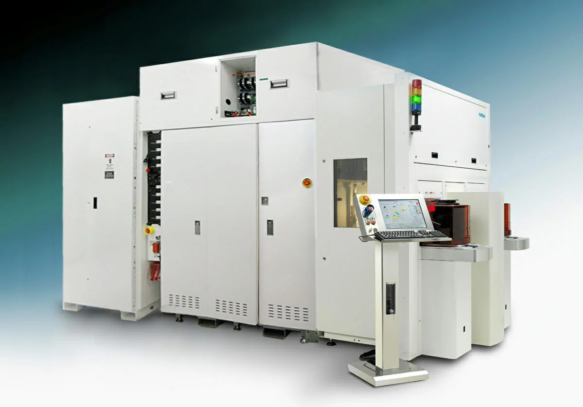
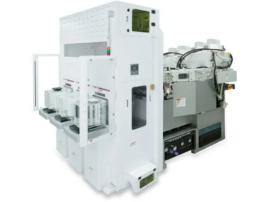
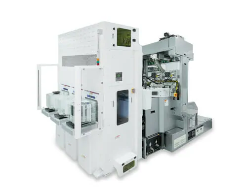
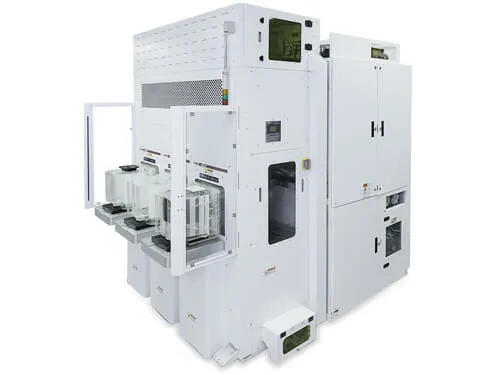
- SUPREMA Dry Strip Systems
- paradigm E Plasma Etch Systems
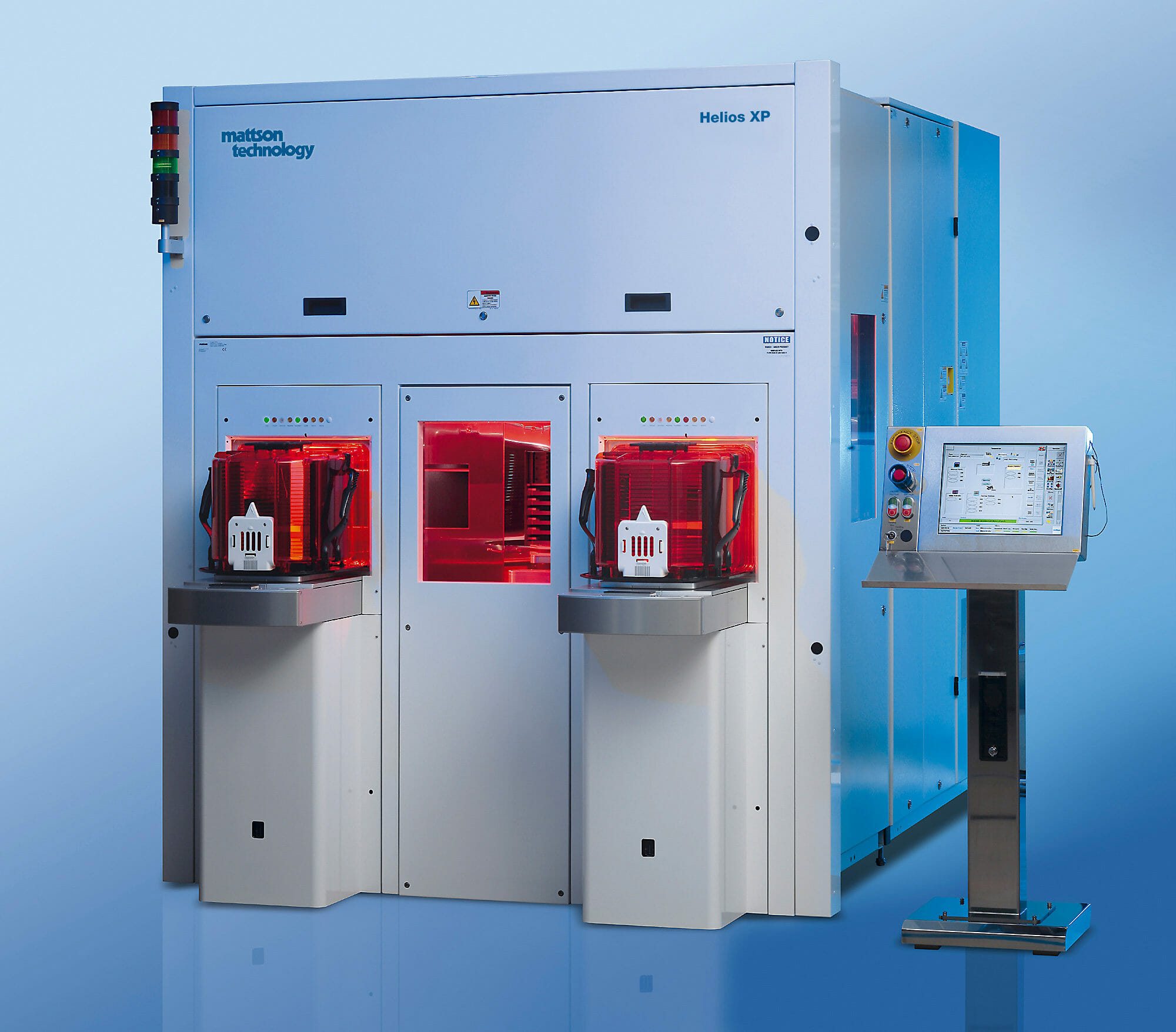
- Helios RTP Systems
- Millios Millisecond Anneal Systems
- Novyka Selective Etch Systems
Dornstadt
DEManufacturing plant
- Materials
- Silicon wafers, photoresist
- Manufacturing of wafer processing systems

Dresden
DESales and service branch (Mattson International GmbH)
Singapore
SGGlobal Operations, Sales & Service
Hsinchu City
TWSales and service
Tokyo
JPSales and service
Systems and Equipment
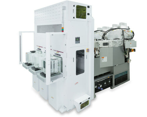
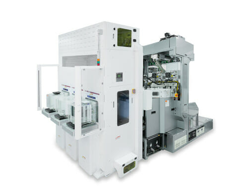
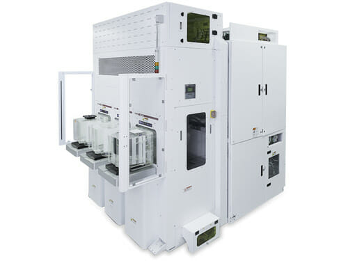
Inside the production

Industries
Processes & technical limits
| Processes | Tolerance | Max. part | Weight | Lot size | Materials |
|---|---|---|---|---|---|
| Dry Strip (Photoresist Strip)Surface | – | – | – | – | Silicon wafers, Photoresist, Hardmask materials, ARC |
| Plasma Etch (ICP)Surface | – | – | – | – | Si, SiN/Oxide, Poly, ONO, BARC, Color filter/lens materials |
| Surface Treatment and Ultra-Selective Materials Removal (Atomic Surface Engineering, NovykaSurface | – | – | – | – | Dielectrics, Conductive materials |
| Rapid Thermal Processing (RTP, double-side heating)Heat treatment | – | – | – | – | Silicon wafers, Nickel/Titanium/Cobalt silicide |
| Millisecond Anneal & Silicidation (Millios)Heat treatment | – | – | – | – | Silicon wafers, Nickel silicide, Titanium silicide, High-k materials |
| Radical Enhanced Thermal Treatment (RETT, Interface Treatment)Heat treatment | – | – | – | – | – |
10 Anlagen & Maschinen
| Machine | Manufacturer / model | Quantity | Working area | Year built | Site |
|---|---|---|---|---|---|
| ICP Plasma Etch System | Mattson Technology paradigm E XP | – | 200/300 mm wafers (derived) | – | – |
| ICP PAD Etcher | Mattson Technology paradigm E PAD | – | – | – | – |
| Plasma Dry Strip System | Mattson Technology SUPREMA | – | – | – | – |
| Dry Strip / Etch Platform (200/300 mm Bridge Tool) | Mattson Technology Aspen III | – | 200 mm / 300 mm wafers; warped wafers > 5 mm | – | – |
| Dry Strip System | Mattson Technology Aspen II | – | Wafers 100/150/200 mm; temperature range 100°C to 250°C | – | – |
| Plasma Strip and Semi-Critical Etch System | Mattson Technology Alpine | – | – | – | – |
| Selective Etch System | Mattson Technology Novyka | – | – | – | – |
| RTP System (Double-Side Heating) | Mattson Technology Helios XP | – | 300 mm wafers (derived); temperature range 200°C to 1300°C | – | – |
| RTP System (200 mm) | Mattson Technology Helios C200 | – | 200 mm wafers; temperature range 200°C to 1300°C | – | – |
| Millisecond Anneal System (Argon Arc Lamp) | Mattson Technology Millios | – | Process range 250°C to 1050°C; max. temperature step 600°C; Emissivity 0.2 to 0.9 | – | – |
Additional services
Quality
Mattson Technology operates according to a global quality management system certified to ISO 9001:2015, supplemented by ISO 14001:2015 (environment) and ISO 45001:2018 (occupational health and safety). Continuous improvement, root cause analysis and supplier partnerships are part of the system.
| Evidence | Mattson Technology (global) |
|---|---|
| ISO 9001:2015 | |
| ISO 14001:2015 | |
| ISO 45001:2018 |
History
- 1988
Founded in Fremont, California; entered the market as a leading supplier of dry strip equipment, later expanded to include Plasma Etch, Rapid Thermal Anneal and Millisecond Anneal
- 1990
Introduction of the Aspen II system
- 2023
Restructuring as a Corporation (Delaware)