
Manufacturing custom high-technology printed circuit boards and embedding solutions from the initial idea to volume production.

Schweizer Electronic AG
Schramberg (DE) · Jintan (CN) · Suzhou (CN) · Singapore (SG) · Dunningen (DE)New on Amplifa
About Schweizer Electronic AG
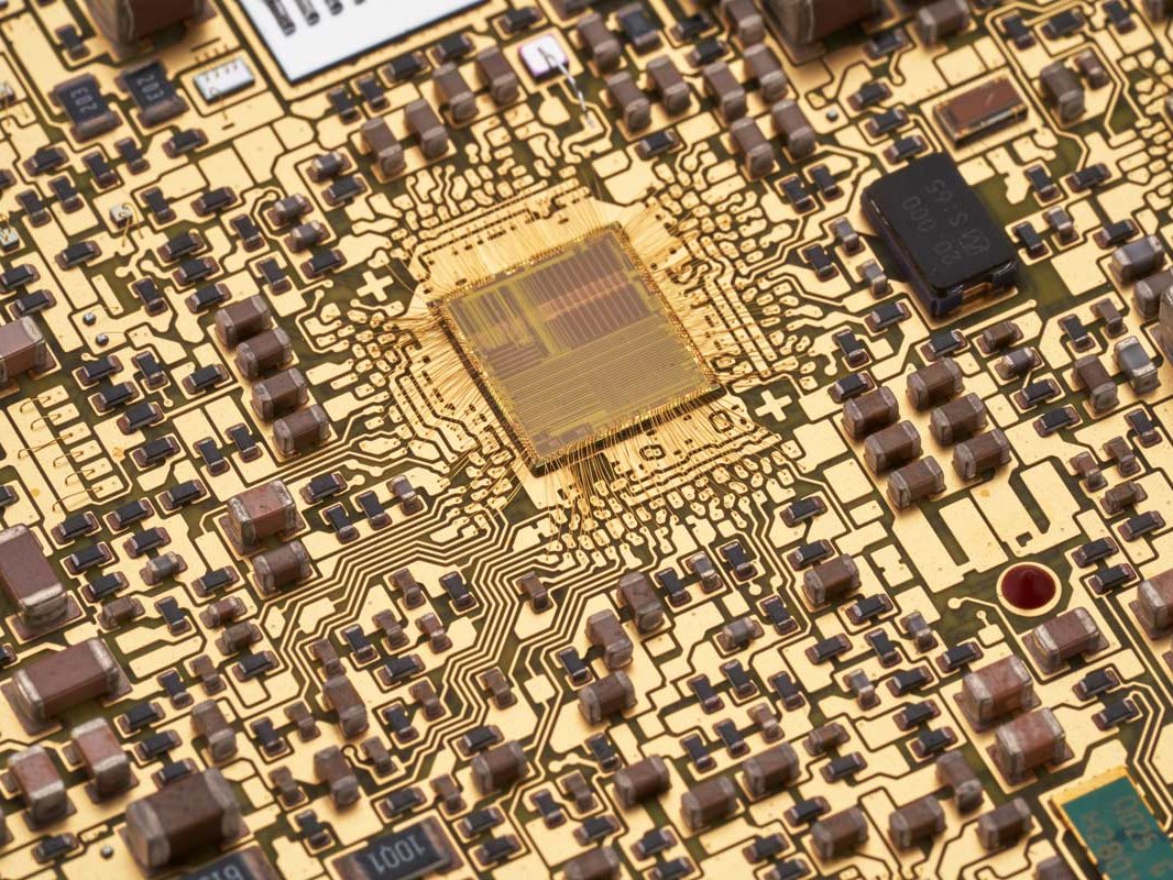
Schweizer Electronic AG is a family-owned manufacturer of custom printed circuit boards and embedding solutions headquartered in Schramberg in the Black Forest. Founded in 1849, the company produces a broad technology portfolio ranging from simple multilayers and complex HDI circuits to thick-copper PCBs with current-carrying capacity of several hundred amperes, inlay boards, RF PCBs up to 77 GHz and p² Pack embedding solutions with integrated power semiconductors. To manufacture the predominantly copper-based traces, the company uses galvanic and chemical baths, laser drilling for microvias and chemical metallization processes such as ENIG and ENEPIG/ENEPAG. SCHWEIZER PCBs are found in demanding applications in the automotive industry, aerospace, industrial and medical technology as well as in telecommunications and computing. Production takes place at the high-tech manufacturing sites in Schramberg (22,500 m² of production and warehouse space) and Jintan/China (90,000 m² of production space), complemented by sales and development centers in Singapore and Suzhou. The company's shares are traded on the Frankfurt and Stuttgart stock exchanges.
- Site
- Schramberg
- Processes
- Multilayer PCBs, HDI PCBs, Thick-copper PCBs (copper 70–400 µm, up to four inner layers of 400 µm, current-carrying capacity, Combi Board, Impedance PCBs (impedance requirements), Inlay Board (copper inlays up to 2 mm thickness, current peaks well above 1,000 A), Bond PCBs (bare die), Embedded Antenna
- Materials
- FR4, Copper, Copper inlay, IMS base material (Insulated Metal Substrate), High-frequency base material (e.g. Teflon), Silicon carbide (SiC semiconductor), Nickel, Gold
- Certificates
- ISO 9001, ISO/TS 16949, ISO 14001, ISO 50001, EN 9100 (DIN ISO EN 9100), NADCAP accreditation, IATF 16949, EN 9100
- Founded
- 1849
- Industries
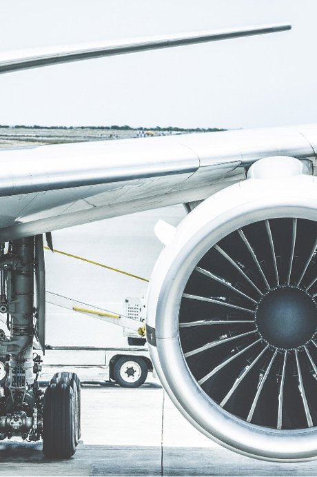
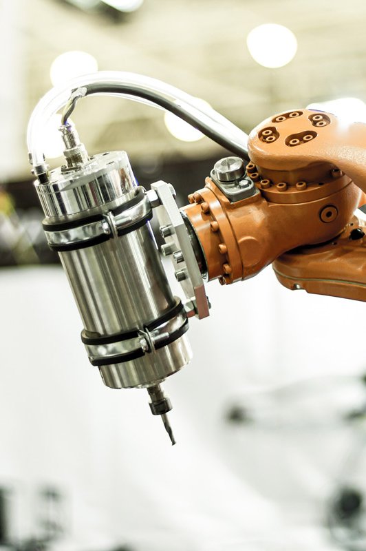
- Automotive, Aerospace, Industrial & Medical technology, Communication & Computing, Power generation and distribution, Solar
- 01
Consulting on layout, layer stack-up and material selection
- 02
Design Rule Check and technical simulation
- 03
PCB manufacturing (drilling, galvanic and chemical baths,
- 04
Laboratory testing and quality control
- 05
Delivery from prototype to volume production
Materials & Processes
FR4
Standard base material for multilayer, HDI, impedance and FR4-flex PCBs.
Copper (thick copper)
Copper thicknesses from 70 to 400 µm for high-current PCBs with current-carrying capacity of several hundred amperes.
Copper inlay
Copper inlays up to 2 mm in thickness enable current peaks well above 1,000 amperes with maximum heat dissipation.
IMS base material
Insulated Metal Substrate with a full-surface copper carrier plate for high thermal conductivity, e.g. for high-power LEDs.
High-frequency base material (e.g. Teflon)
Stable dielectric properties for RF PCBs up to 77 GHz, usually manufactured as hybrid circuits.
Silicon carbide (SiC)
Wide-bandgap semiconductors for p² Pack embedding with voltages up to 1200 V and junction temperatures above 200 °C.
ENIG (chemical Ni/Au)
Chemical metallization with nickel/gold as the final surface finish of the PCB.
ENEPAG (NiPdAu)
Nickel-palladium-gold surface finish for demanding applications.
Chemical tin
Chemical tin as the final surface finish of the PCB.
Chemical silver
Chemical silver as the final surface finish of the PCB.
Galvanic NiAu
Electroplated nickel/gold surface finish for fine and demanding requirements.
Locations

Schramberg
DEHeadquarters, high-tech PCB manufacturing, innovation center
- Part weight / size
- Max. PCB size 575 x 583 mm, thickness 0.4–3.8 mm
- Lot size
- Prototype to volume production
- Materials
- FR4, copper, high-frequency base material, IMS, SiC
- PCB manufacturing line / high-tech production
- Climate chambers (reliability testing)
- Thermal shock chambers
- SEM microscopy
- Galvanic and chemical baths
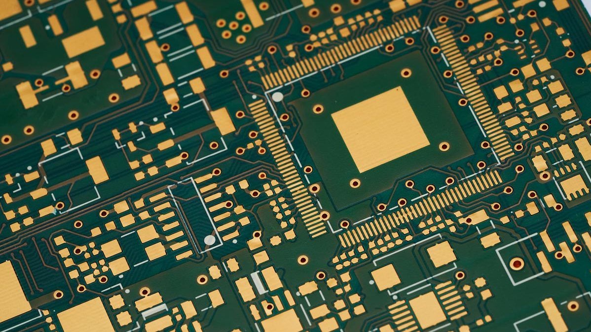
Jintan (Changzhou)
CNProduction site for power electronics and MOSFET embedding (automotive)
- Lot size
- Small, medium and large series
- Materials
- Copper, silicon carbide, FR4
- High-tech production for power electronics and MOSFET embedding
- Laser drilling machine (microvia)
Suzhou
CNSales office (Schweizer Trading Suzhou Co. Ltd., founded 2023)
Singapore
SGPurchasing & Sales (Schweizer Electronic Singapore Pte. Ltd., founded 2012)
Dunningen
DEFactory (inaugurated 1967)
Components & Technologies
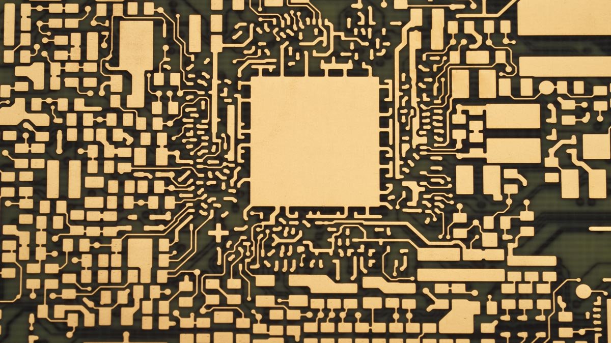
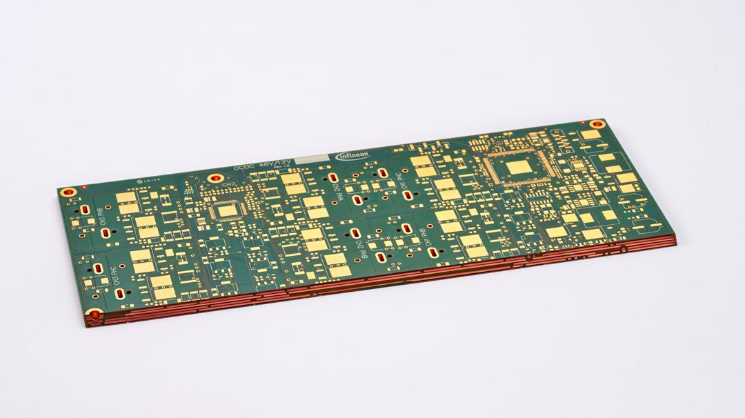
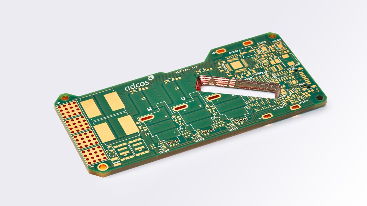
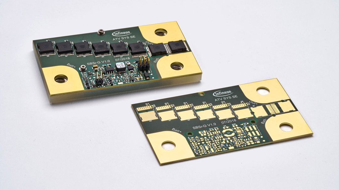
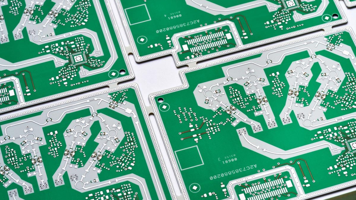
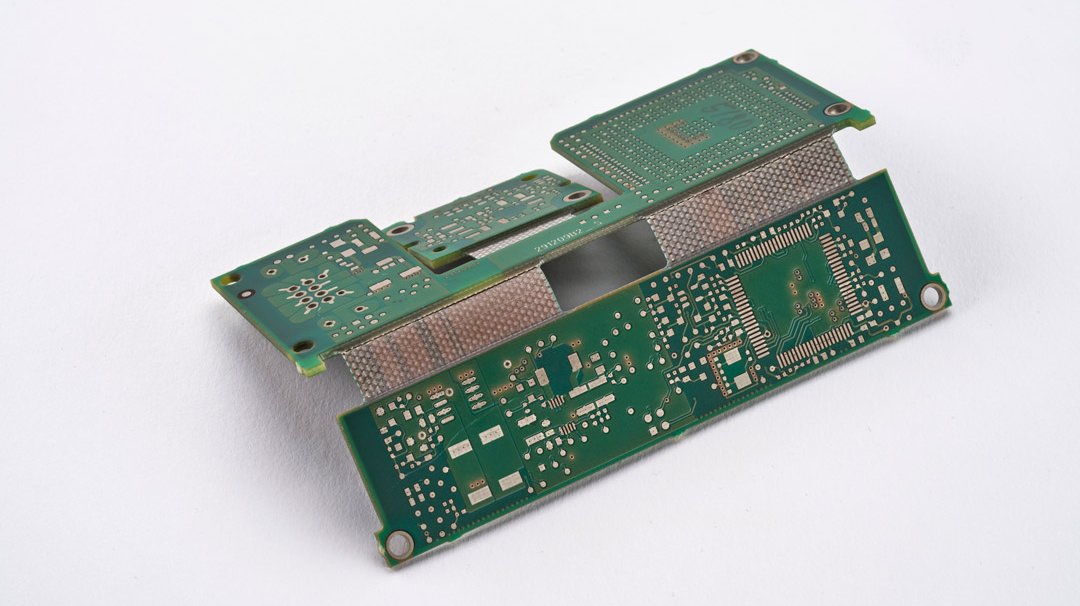
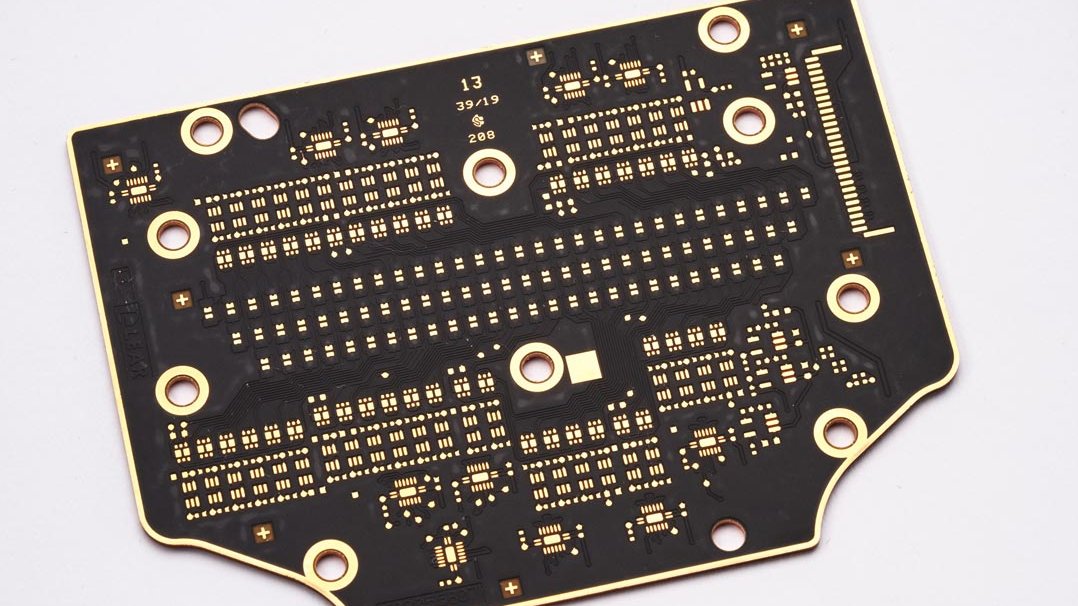
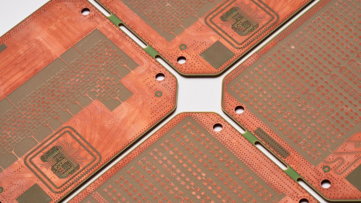
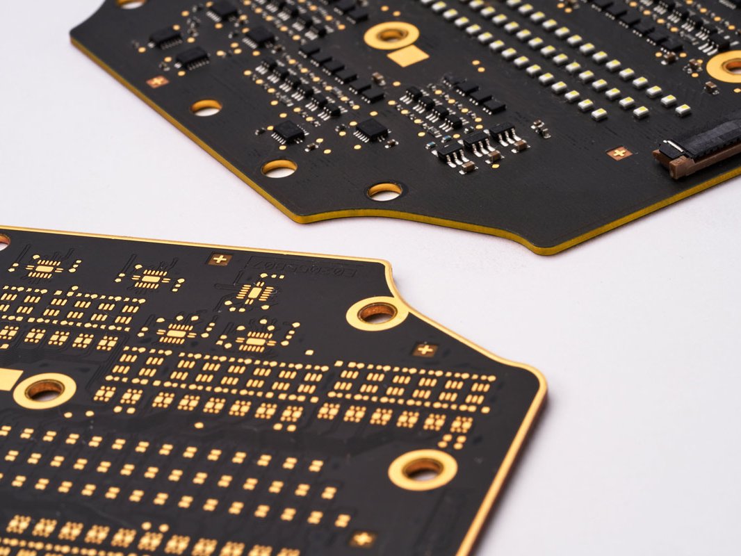
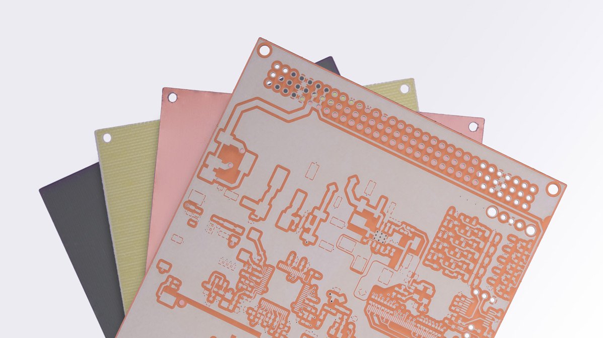
Inside the production
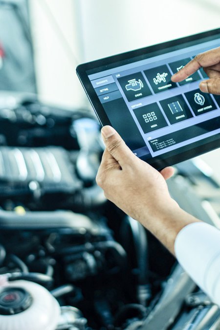
Industries
Processes & technical limits
| Processes | Tolerance | Max. part | Weight | Lot size | Materials |
|---|---|---|---|---|---|
| Multilayer PCBsEngineering | – | 575 mm × 583 mm | – | – | FR4 |
| HDI PCBsEngineering | – | – | – | – | FR4 |
| Thick-copper PCBs (copper 70–400 µm, up to four inner layers of 400 µm, current-carrying capacityEngineering | – | – | – | – | Copper |
| Combi BoardEngineering | – | – | – | – | FR4 |
| Impedance PCBs (impedance requirements)Engineering | – | – | – | – | FR4 |
| Inlay Board (copper inlays up to 2 mm thickness, current peaks well above 1,000 A)Engineering | – | – | – | – | Copper |
| Bond PCBs (bare die)Engineering | – | – | – | – | – |
| Embedded AntennaEngineering | – | – | – | – | – |
| RF PCBs 6-24 GHzEngineering | – | – | – | – | High-frequency base material, Teflon |
| RF PCBs 77 GHz (high-frequency PCBs up to 79 GHz, hybrid circuits)Engineering | – | – | – | – | High-frequency base material |
| p² Pack semiconductor embedding 48 V (junction temperatures up to 175 °C, wide-bandgap > 200 °C,Engineering | – | – | – | – | Silicon carbide |
| FR4-flex PCBs (flexible)Engineering | – | – | – | – | FR4 |
| Cu-IMS (Insulated Metal Substrate)Engineering | – | – | – | – | Copper, IMS base material |
| T² technology (thick-copper technology with pre-filled etched trenches)Engineering | – | – | – | – | Copper |
| Surface technology: chemical metallization (ENIG, ENEPIG/ENEPAG) and galvanic processesSurface | – | – | – | – | Nickel, Gold, Palladium, Tin, Silver, Copper |
| Laser drilling of microvias (minimum 100–110 µm drill diameter)Engineering | – | – | – | – | – |
| Layer stack-up, layout and technology consultingEngineering | – | – | – | – | – |
| Design Rule CheckTesting | – | – | – | – | – |
| Thermal simulation / thermal management / impedance and RF calculationsEngineering | – | – | – | – | – |
| Laboratory testing: climate chambers, thermal shock chambers, cross-section analyses, SEMTesting | – | – | – | – | – |
| Galvanic and chemical baths for manufacturing copper tracesSurface | – | – | – | – | Copper |
7 Anlagen & Maschinen
| Machine | Manufacturer / model | Quantity | Working area | Year built | Site |
|---|---|---|---|---|---|
| PCB manufacturing line / high-tech production (production area 22,500 m², usable area approx. | Schweizer Electronic AG | – | – | 1979 | Schramberg, Germany |
| High-tech production for power electronics and MOSFET embedding (production area 90,000 m²) | Schweizer Electronic (Jiangsu) Co., Ltd. | – | – | 2019 | Jintan, China |
| Climate chambers (reliability testing) | – | – | – | – | Schramberg |
| Thermal shock chambers | – | – | – | – | Schramberg |
| SEM microscopy | – | – | – | – | Schramberg |
| Laser drilling machine (microvia) | – | – | – | – | Schramberg / Jintan |
| Galvanic and chemical baths | – | – | – | – | Schramberg |
Additional services
Quality & Certifications
SCHWEIZER's laboratories are equipped with extensive measuring and analysis equipment, including climate chambers, thermal shock chambers, cross-section analyses, SEM microscopy, FTIR spectroscopy as well as tests for ionic contamination, dielectric strength and IST test measurements of CTE and Tg. The company is certified, among others, to ISO 9001, ISO 14001, ISO 50001 and DIN ISO EN 9100 and holds a NADCAP accreditation.
| Evidence | Schramberg | Jintan (Changzhou) |
|---|---|---|
| ISO 9001 | ||
| ISO 14001 | ||
| ISO 50001 | ||
| IATF 16949 | ||
| EN 9100 | ||
| NADCAP accreditation |